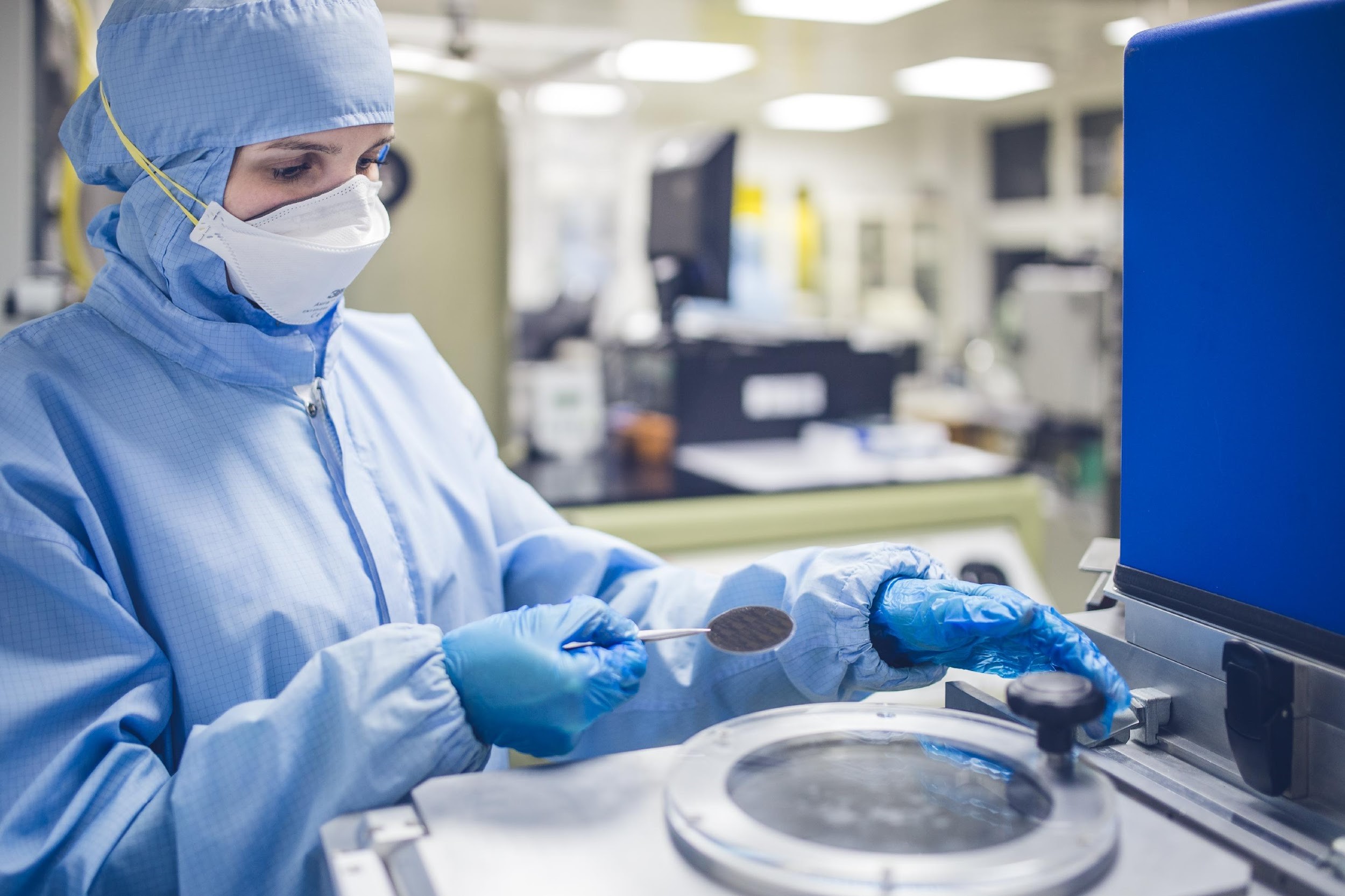
As part of our work, the structure of the optical fiber is most often modified by applying a thin layer of material (from a few to several hundred nanometers) to the surface of the optical fiber in a highly controlled manner. The presence of the layer allows to obtain a specific optical effect (usually resonance) and to optimize the sensitivity. In our laboratories, thin layers are obtained by magnetron sputtering, plasma enhanced chemical vapor deposition (PECVD) and atomic layer deposition (ALD). The thin films we manufacture include, among others, carbon materials, compounds of titanium, aluminum, hafnium, tin, indium, tantalum, zirconium, zinc and silicon. We embed metals, dielectrics and semiconductors, also in the form of multi-layer systems with a highly controlled structure. Metals and semiconductors, apart from obtaining optical interactions, also allow the integration of electrical and electrochemical measurements within one sensor.